TOUCH AND FEEL AT THE NANOSCALE
SOLUTIONS
COMPLETE SENSOR SOLUTIONS
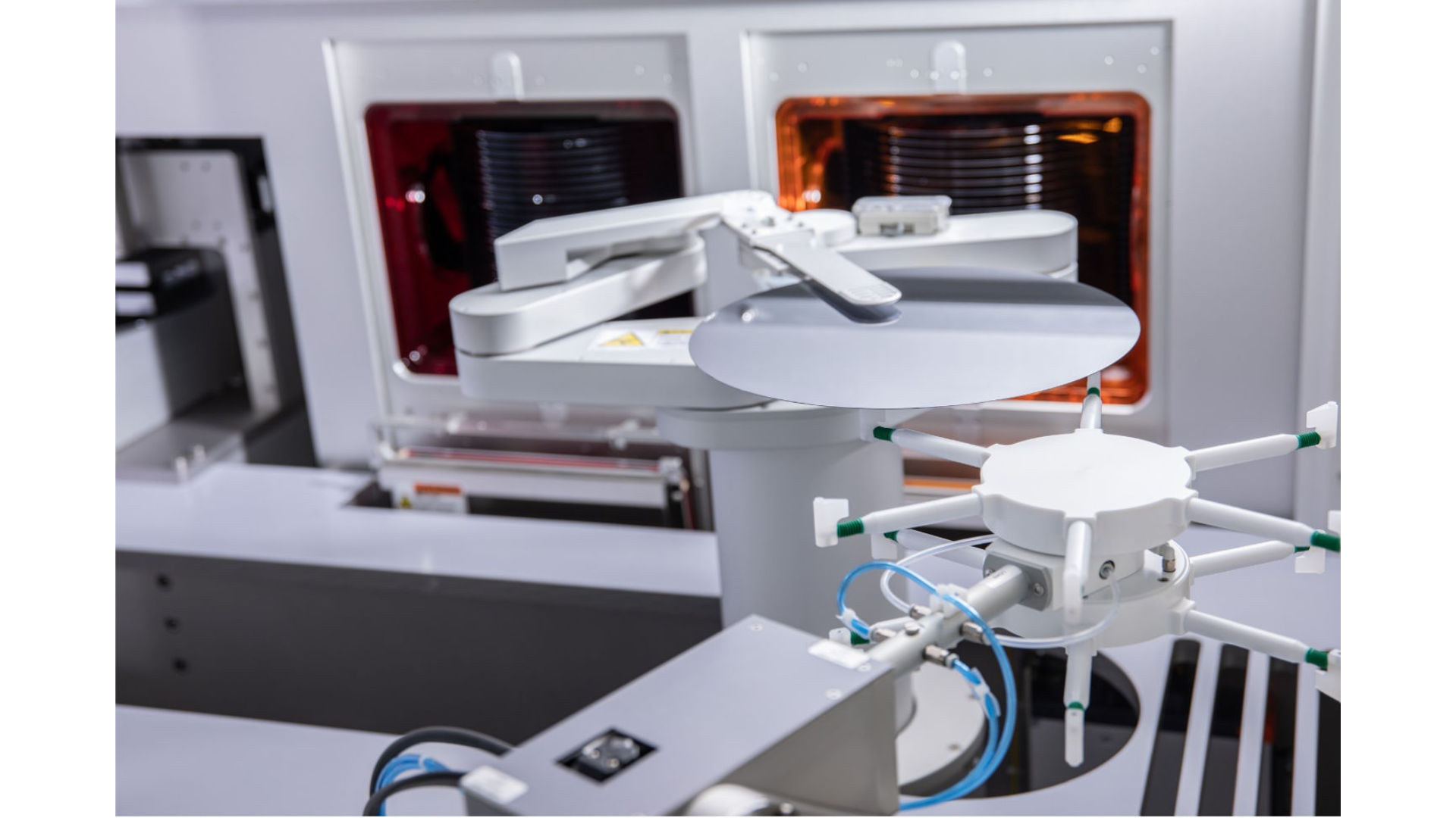
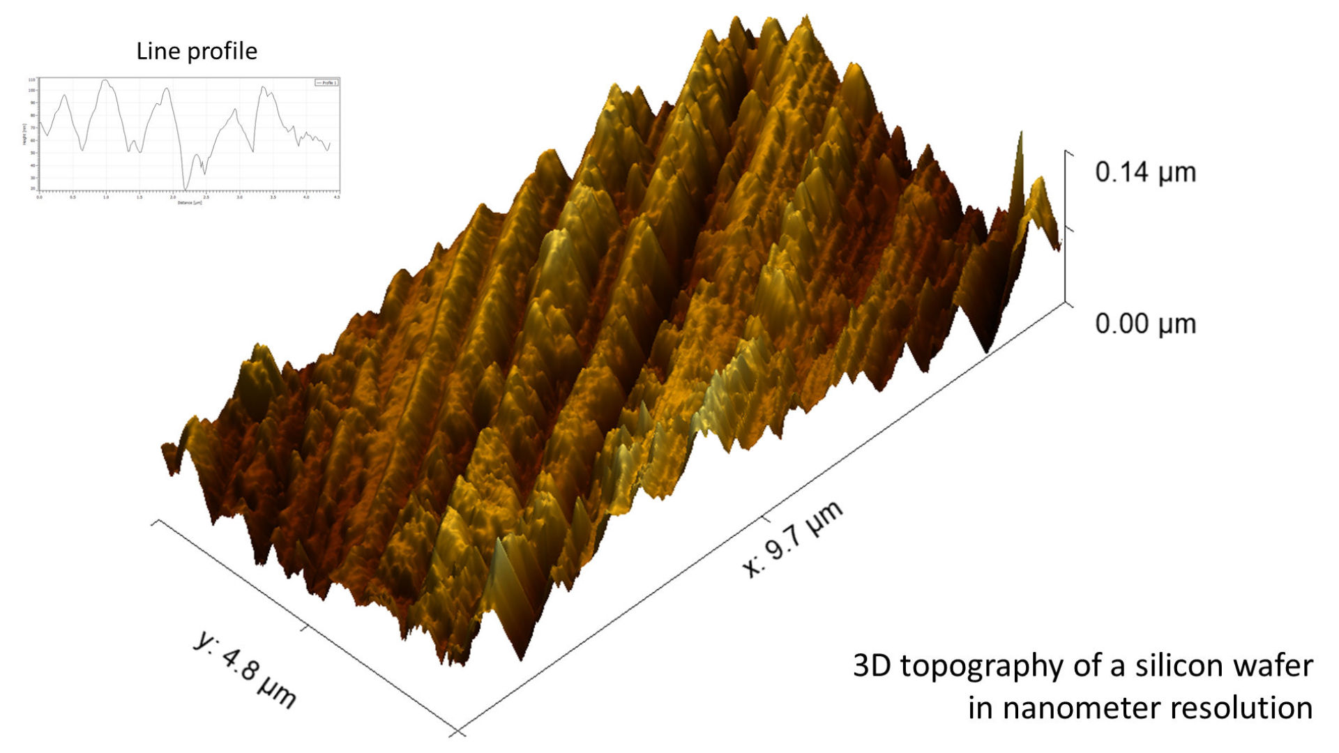
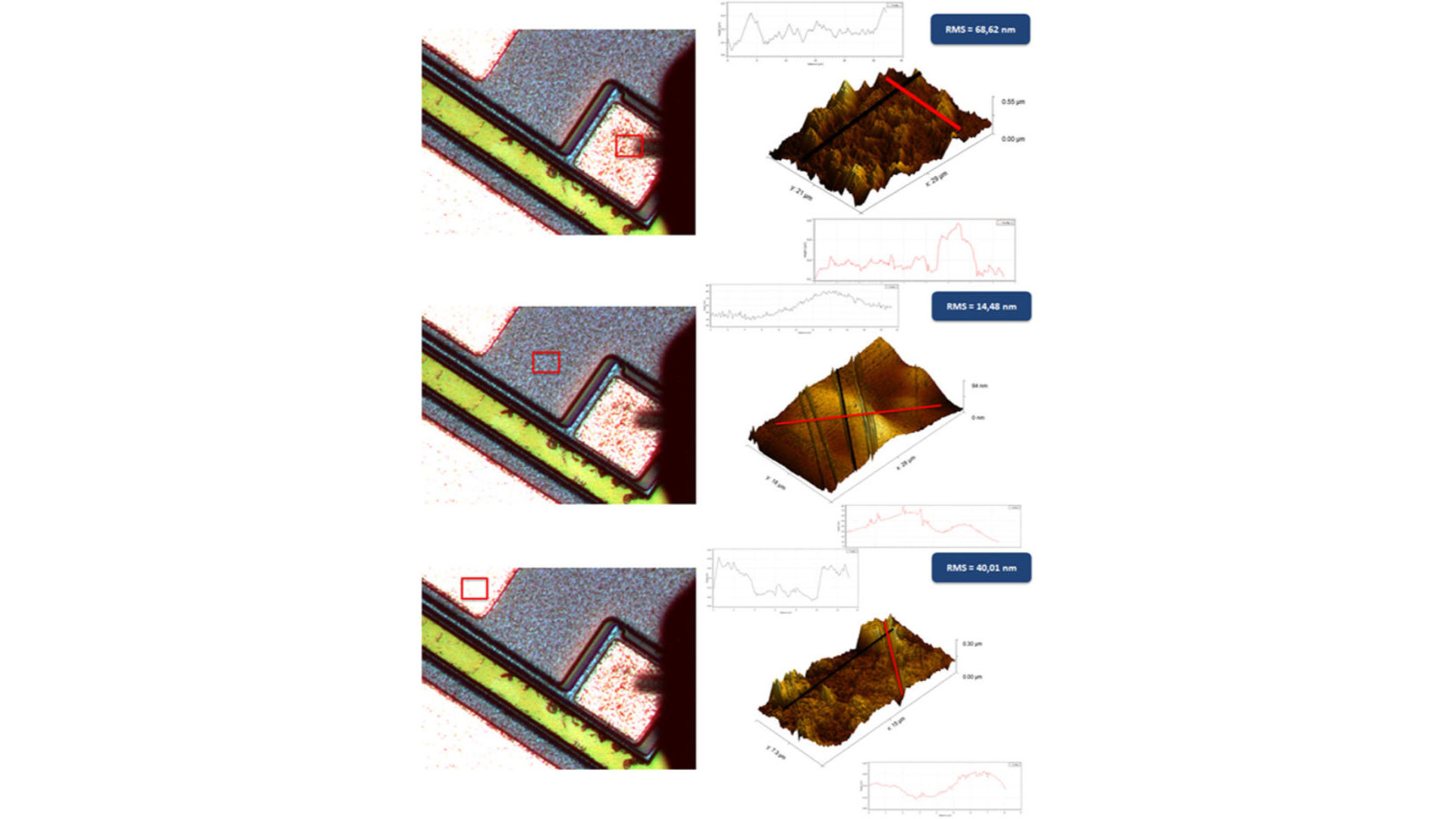
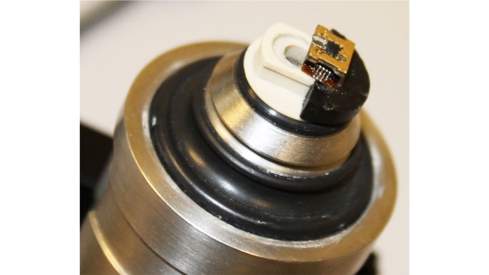
NASSWAF (Nano Surface Scanner for Wafers) project
The aim of the NASSWAF (Nano Surface Scanner for Wafers) project is the development of a roughness measurement module (RMM) for the integration into the „Ultra-Thin Wafer Handling and Roughness Control System“ of the Singapore company NexGenWS. This integrated wafer handling and roughness control system will be the first solution available in the market that combines Ultra-Thin Wafer Processing and an In-Line Surface Roughness Control System in a Single Wafer WetChemical Processing Equipment for the semiconductor industry. Both systems will be combined into one functional unit and integrated into NexGen‘s Wafer Systems existing product line of processing equipment.
Artificial Intelligence-driven algorithms will analyze the roughness data as well as other process-specific parameters and control the individual modules that are part of this system to perform proactively and predictive process control for semiconductor surface treatment processes. The individual modules will consist of mechanical, electronics, software and mechatronic systems that will be controlled by one central controller (host computer).
The outcome for the semiconductor industry NexGen customers will be versatile. Device manufacturers will be able to perform the critical process of the surface roughness measurement right in the equipment that performs the surface conditioning process for the first time. It will also be the first time that this type of manufacturing equipment will be able to actively control and optimize the roughness of the wafer based on real-time roughness measure-ments and process parameters. The system will be self-learning without any external (human) intervention based on the data that the system generates, collects and analyses by itself.
In-Line roughness control will result in significantly better device quality and performance, manufacturing yields, less waste and optimized usage of the chemical substances, which goes along with massive cost savings for the device manufacturer and a positive environmental impact.
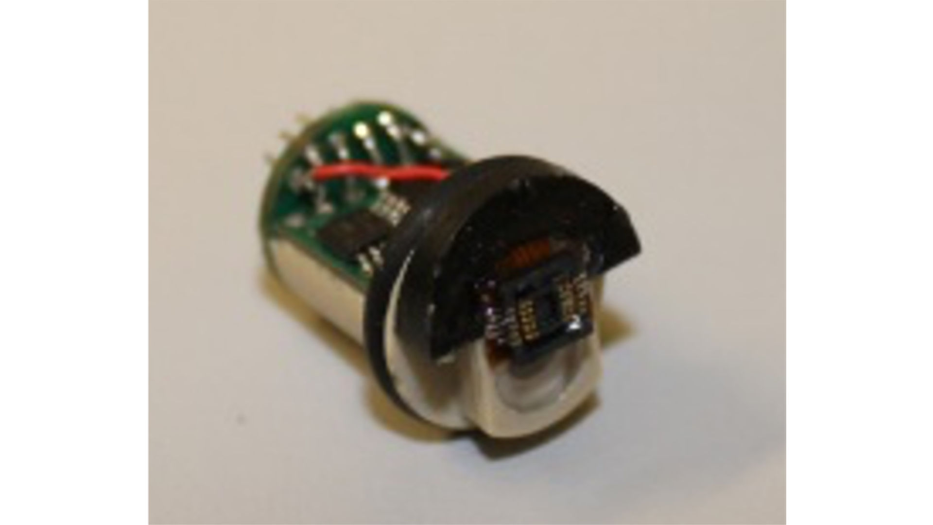
SENSOR MODULES
Adapters enable all electric measurements with standard AFMs:
Keysight Addon 5500:
The Keysight 5500 add-on was developed for the use of self-sensing technology in a regular optical atomic force microscope. This AFM is widely used in research and industry and can be converted from an optical AFM to a purely self-sensing All Electric AFM using the add-on. There is no damage to the microscope, so you can switch between optical and self-sensing mode at any time. This eliminates the need to purchase an expensive AFM and enables laser-free measurements using your existing microscope with many advantages for various applications.
Bruker Addon:
Bruker is world’s leading AFM manufacturer. Since Bruker’s AFMs are exclusively designed for optical cantilevers, some applications for these products are fundamentally ruled out. The implementation of an adapter enables the use of self-sensing technology in a Bruker AFM. This extends the application range to measurements in non-transparent liquids and facilitates easy cantilever handling. This can be of great advantage especially in the fields of biology, biochemistry and cell research, without having to forego the advantages of conventional optical cantilevers.
STARTER KIT
Self-Sensing Starter Kit
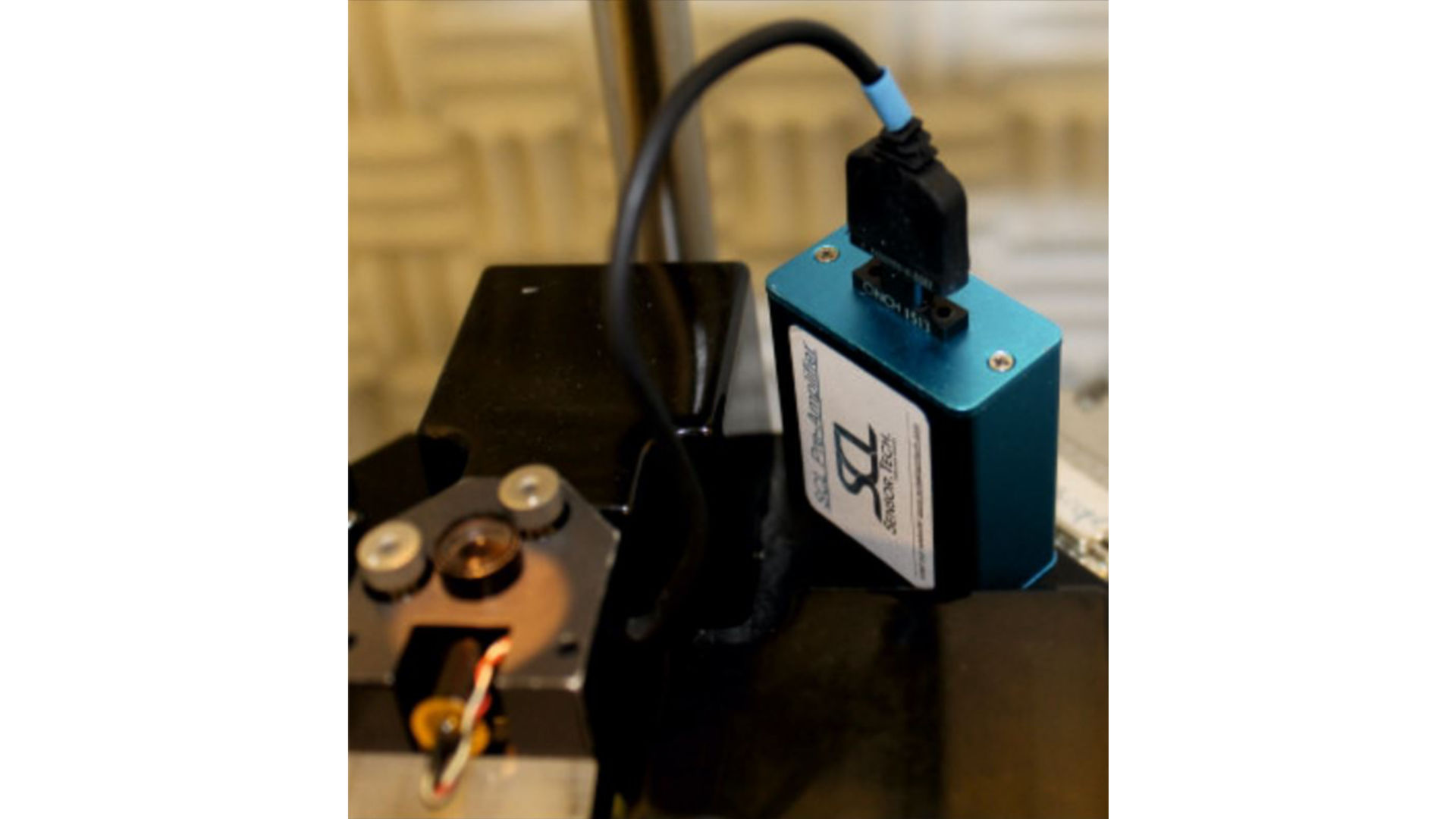
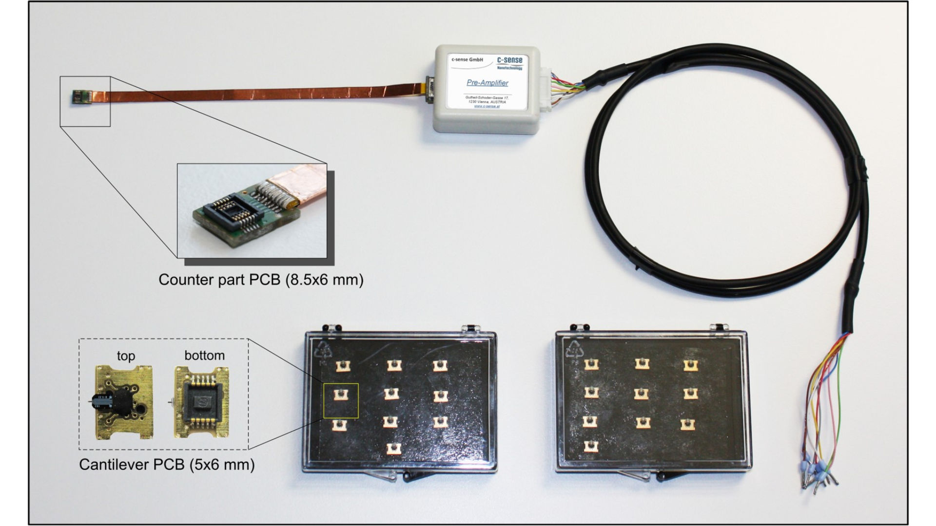
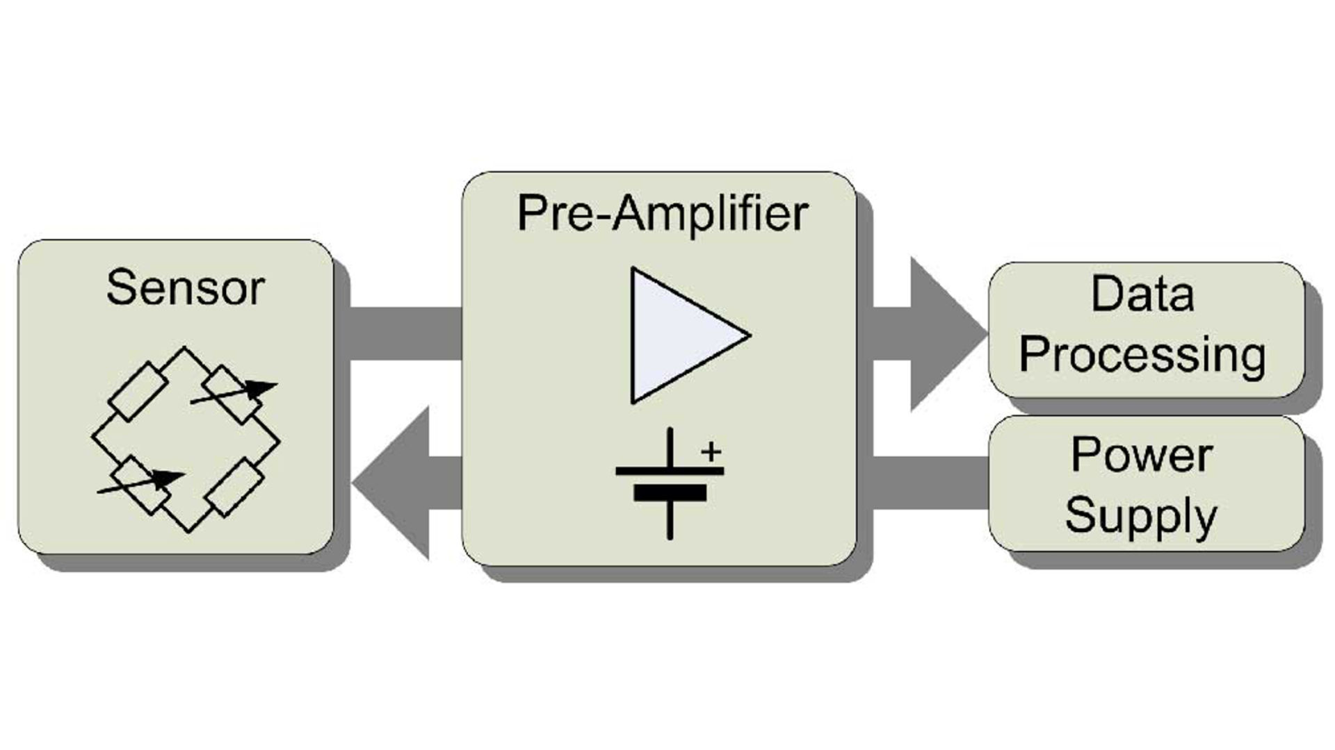
The Self-Sensing Starter Kit includes a pre-amplifier, connection cables and 10 pieces of cantilevers to get easily started. The core element of c-sense self-sensing starter kit is the pre-amplifier. It supplies a Wheatstone bridge based sensor with a stable and low noise reference voltage and amplifies the bridge output signal.
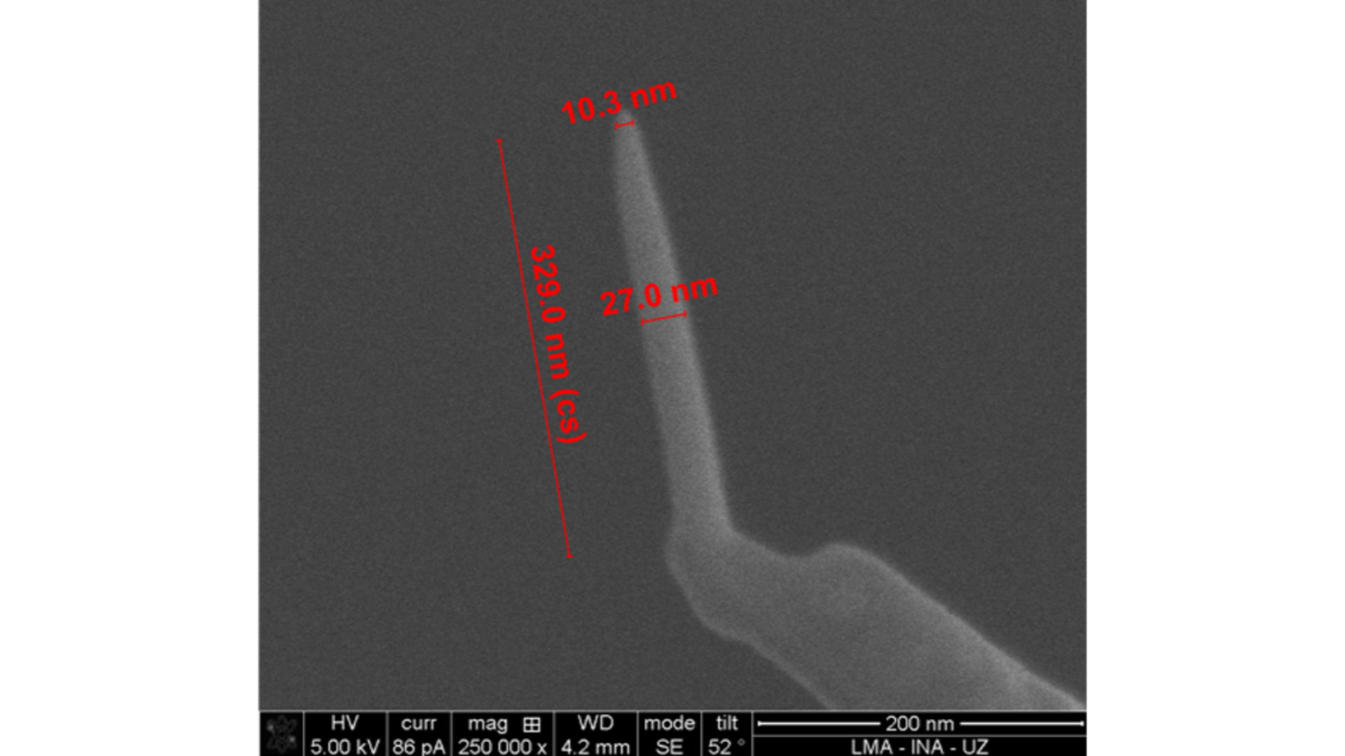
CUSTOMIZED CANTILEVER SENSORS
In order to guarantee the greatest possible flexibility for individual problems of our customers, c-sense offers customized cantilevers. We are also open to potential new cantilever developments. Do not hesitate to contact us.
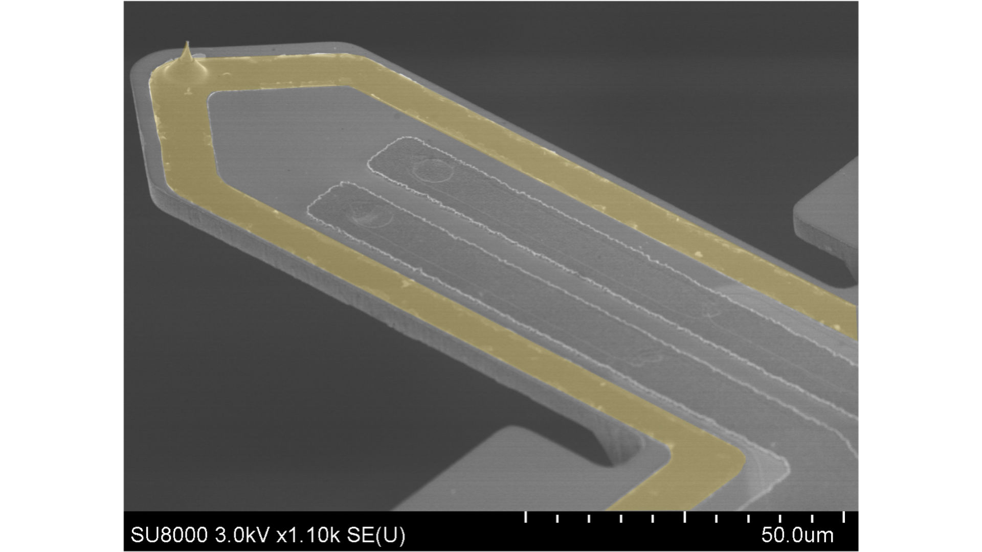
Conductive Cantilevers
To perform conductivity measurements and electrical probing c-sense offers gold coated cantilevers that allow for measurements of small areas and are further suitable for methods like Tip Enhanced Raman Spectroscopy (TERS). For enhanced stability tips grown out of tungsten or platinum/gold are also available.
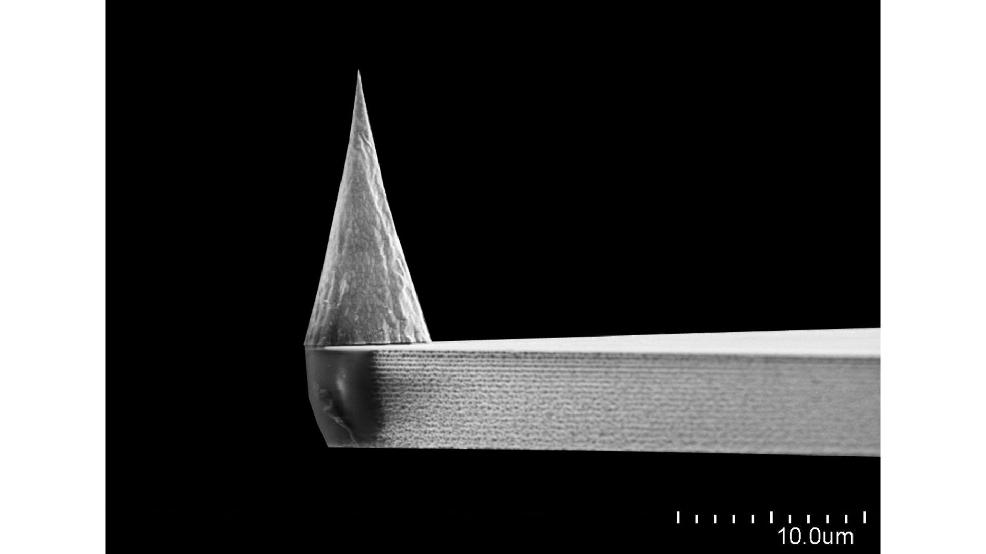
Diamond Tips
For Nanoprobing, scratching experiments and highly demanding topography measurements cantilevers with single crystal diamond tips (SCD) are the perfect fit due to high stability, hardness and endurance.
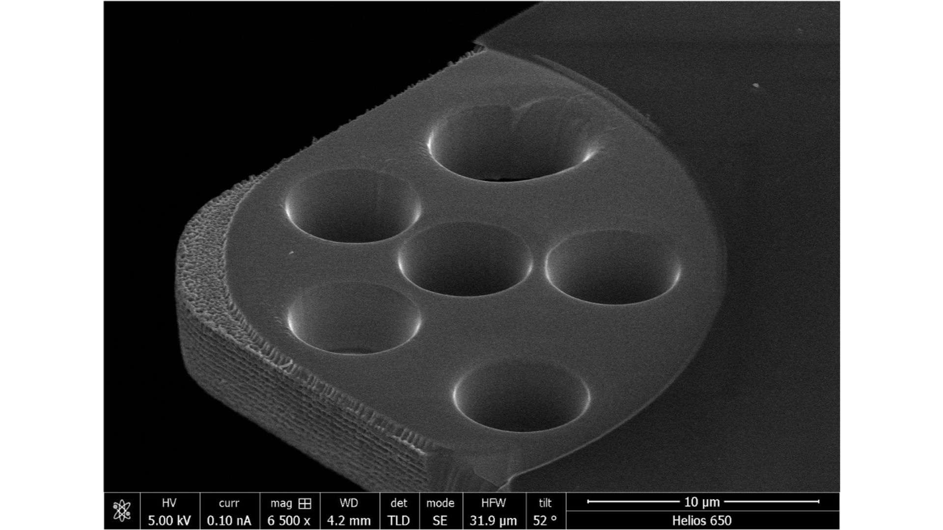
Pierced Cantilevers
Cantilevers can be modified in order to place holes according to our customer’s demands. Exact positioning of the now visible tip becomes possible.
Magnetic Coating of Cantilevers
To perform magnetic measurements we offer cantilevers with magnetic coating or tips grown out of magnetic alloys.
Contact us:
Diese Website ist durch reCAPTCHA geschützt und es gelten die Datenschutzbestimmungen und Nutzungsbedingungen von Google.