Our self-sensing cantilevers are excellent probes for conductive measurements in, e.g., material science and semiconductor failure analysis. Applications include, among others, cAFM, nanoprobing, IV spectroscopy, or SSRM.
In conductive AFM (cAFM), the sharp conductive tips of our self-sensing cantilevers can be used to map topography and current flowing through the sample.
Due to their small tip radii and the integrated force-feedback, our self-sensing cantilevers are an excellent choice for nanoprobing applications even at the latest semiconductor technology nodes such as 5 nm, 3 nm, 2 nm and 1 nm nodes.
In practice
How researchers use it
Example 1: Custom FEBID tips for probing
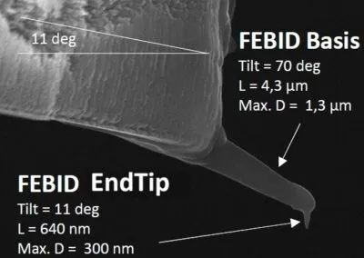
SEM image of a two-stage FEBID tip. Base: 4.3 µm long, maximum diameter 1.3 µm. End tip: 640 nm long, maximum diameter 300 nm. Credit: c-sense
The study. For probing small contacts, tips are written by focused electron beam induced deposition (FEBID). The example shows a two-stage tip: a 4.3 µm long base carrying a 640 nm end tip with a maximum diameter of 300 nm. Length, tilt and tip shape are adapted to the contact that has to be reached.
Where our cantilever is used. The tip is deposited directly onto one of our self-sensing cantilevers, which then provides the force feedback for landing the tip on the contact.
c-sense.
Example 2: A 22 nm conductive tip in constant contact at 4 K
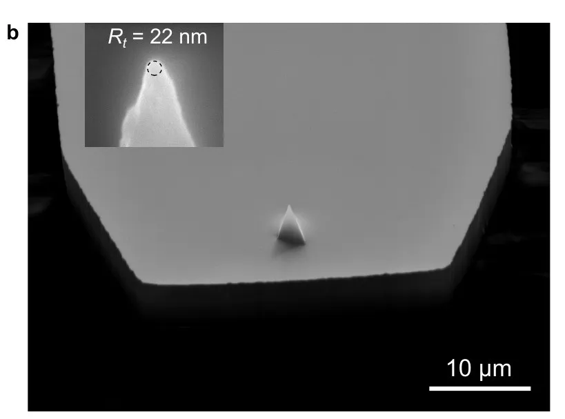
SEM image of the self-sensing cantilever with its conductive tip. Inset: the tip apex with a radius of about 22 nm. Scale bar 10 µm. Credit: Lyu, Vento et al., arXiv:2608.28574 (2026); use with the authors' permission
The study. In the Geneva experiment on quantum emitters, a conductive tip is scanned over the sample at 4 K as a local gate electrode. The tip must stay in contact during line and raster scans without damaging the sample.
Where our cantilever is used. The probe is a self-sensing cantilever with a 100 nm Pt coating and a tip radius of about 22 nm. The Pt coating carries the gate voltage, and the piezoresistive signal is used to hold the contact force constant.
B. Lyu, V. Vento et al., arXiv:2608.28574 (2026). Figure: use with the authors' permission.