Surface height / 3D profile: our self-sensing cantilevers can map roughness, step heights, and general surface features on nanometer scale.
Phase imaging: with our self-sensing cantilevers, surface composition, stiffness variations, or sticky areas in dynamic modes can be identified and differentiated.
In practice
How researchers use it
Example 1: nm roughness on a silicon wafer
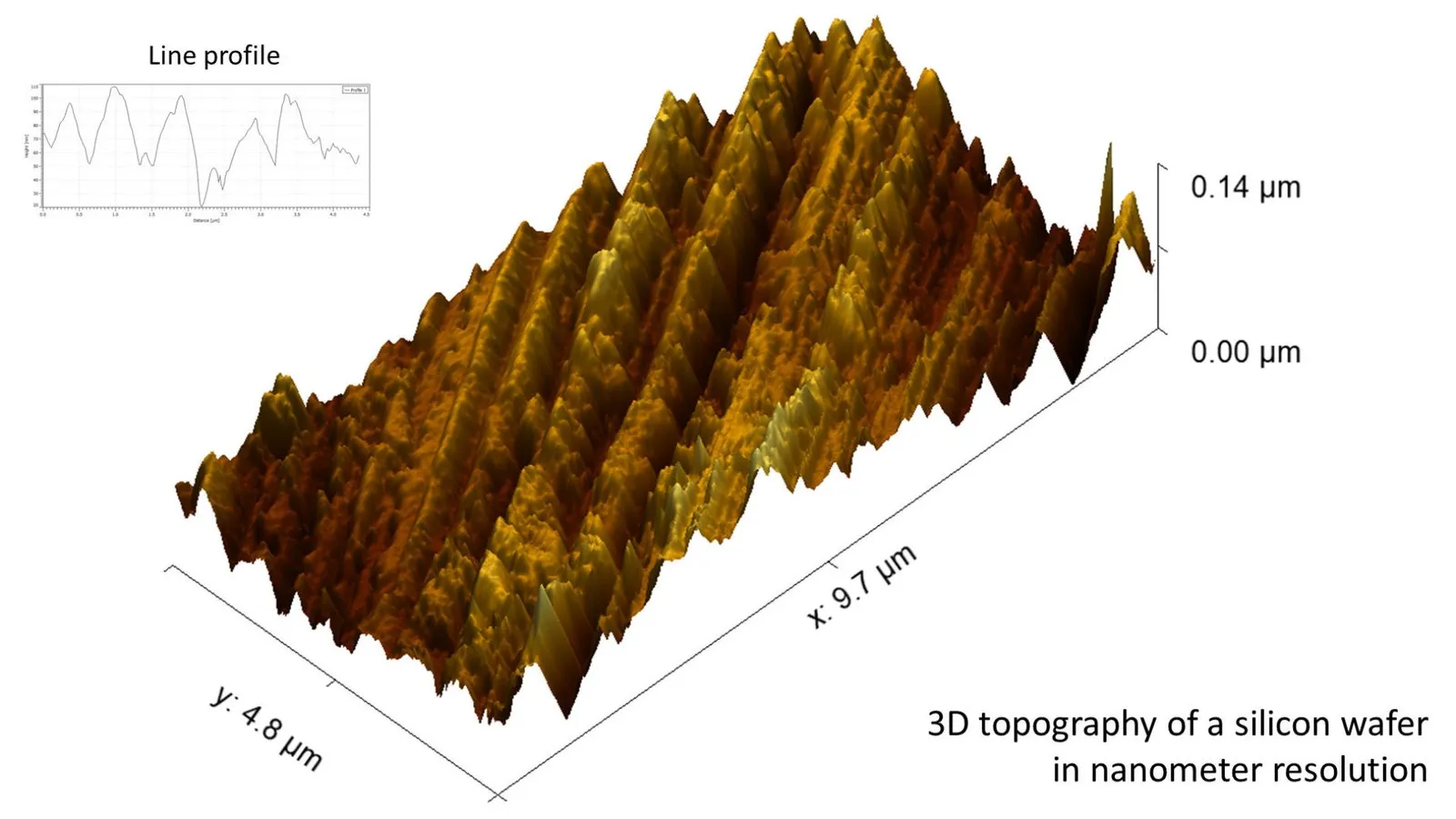
3D topography and line profile of a silicon wafer at nanometre resolution. Scan area 9.7 µm × 4.8 µm, height range 0.14 µm. Credit: c-sense
The study. A silicon wafer surface was scanned to measure its roughness. The result is a line profile and a 3D surface model at nanometre resolution, the kind of measurement used for process control in wafer production.
Where our cantilever is used. A self-sensing cantilever sensor module does the whole measurement: its tip scans the surface and its integrated sensor reads the height electrically, without a laser.
Example 2: An AFM that measures from any direction
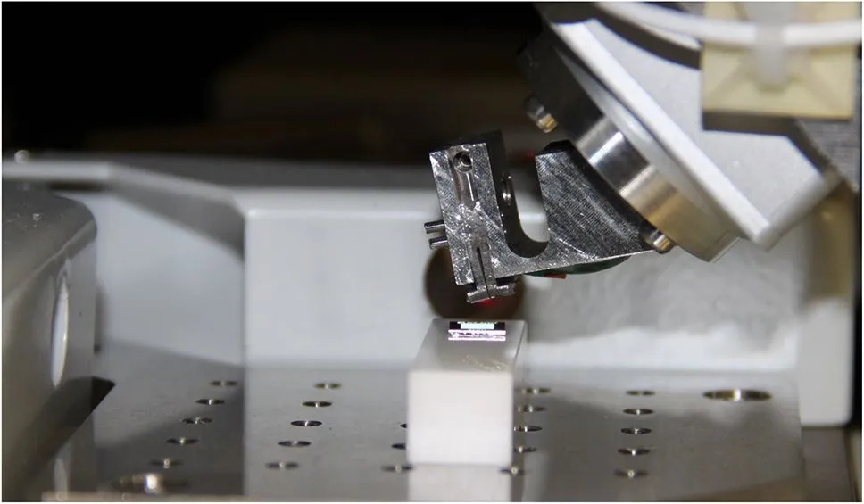
The AFM head with the self-sensing cantilever inside the nano measuring machine NMM-1 at FAU Erlangen-Nürnberg. Credit: Schaude and Hausotte, Nanomanuf. Metrol. 5, 139–148 (2022), CC BY 4.0
The study. The Institute of Manufacturing Metrology at FAU Erlangen-Nürnberg built an AFM whose probe direction can be tilted over a complete hemisphere and integrated it into a nano measuring machine (NMM-1). The aim is to measure microstructures and side walls that a top-down AFM cannot reach.
Where our cantilever is used. Our PRSA self-sensing cantilever (110 µm × 48 µm, silicon tip) with our preamplifier is the probe of this AFM. It senses the deflection and, through its integrated micro heater, also drives its own oscillation, so the head needs neither a laser nor a separate piezo actuator. This is what makes a tilting head possible.
J. Schaude, T. Hausotte, Nanomanufacturing and Metrology 5, 139–148 (2022), doi:10.1007/s41871-022-00143-9. CC BY 4.0.
Example 3: Topography of a graphene membrane inside the SEM
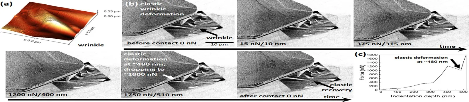
Tapping-mode AFM image of a wrinkle in a suspended few-layer graphene membrane (top left) and SEM images taken while the AFM tip indents the wrinkle. Credit: Hummel et al., Appl. Phys. Lett. 118, 103104 (2021), CC BY 4.0
The study. Researchers at the University of Vienna and GETec Microscopy studied suspended few-layer graphene membranes with an AFM operated inside a scanning electron microscope. The image shows a wrinkle in the membrane in tapping mode, together with SEM images of the same spot.
Where our cantilever is used. The AFM is the AFSEM system, which is built around a self-sensing piezoresistive cantilever. The cantilever sits directly under the SEM objective lens and records the topography; because it needs no optical readout, the AFM fits into a standard SEM chamber.
S. Hummel et al., Applied Physics Letters 118, 103104 (2021), doi:10.1063/5.0040522. CC BY 4.0.
Example 4: Collagen, an insect eye and atomic steps, imaged without a laser
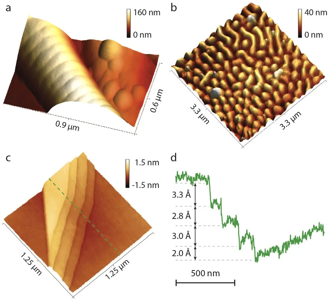
AFM images taken with piezoresistive readout: (a) collagen fibril with 67 nm banding, (b) cornea of a housefly eye with features about 10 nm high, (c) atomic steps on graphite, (d) line profile across the steps with height differences of 2 to 3 Å. Credit: Dukic, Adams and Fantner, Sci. Rep. 5, 16393 (2015), CC BY 4.0
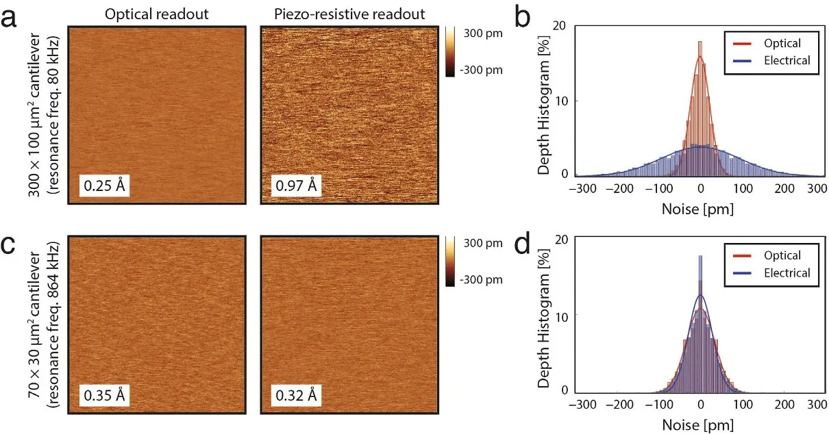
The study. The Laboratory for Bio- and Nano-Instrumentation at EPFL compared piezoresistive readout with the standard optical readout and showed that small self-sensing cantilevers reach the same noise level, about 0.3 Å at 20 kHz bandwidth. They then imaged a collagen fibril (67 nm banding), the cornea of a housefly eye and atomic steps on graphite.
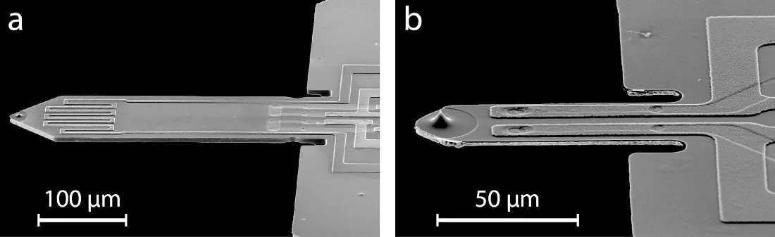
Where our cantilever is used. All images were taken with SCL-Sensor.Tech cantilevers: PRSA 300 µm × 100 µm and PRS 70 µm × 30 µm. The cantilevers were the imaging probes, and their built-in piezoresistive bridge was the readout that the study benchmarks against the laser.
Noise images and histograms for optical and piezoresistive readout. 300 × 100 µm cantilever: 0.25 Å optical, 0.97 Å piezoresistive. 70 × 30 µm cantilever: 0.35 Å optical, 0.32 Å piezoresistive. Credit: Dukic, Adams and Fantner, Sci. Rep. 5, 16393 (2015), CC BY 4.0 SEM images of the silicon piezoresistive cantilevers used: (a) 300 × 100 µm, (b) 70 × 30 µm. Credit: Dukic, Adams and Fantner, Sci. Rep. 5, 16393 (2015), CC BY 4.0
M. Dukic, J. D. Adams, G. E. Fantner, Scientific Reports 5, 16393 (2015), doi:10.1038/srep16393. CC BY 4.0.