KPFM and EFM yield quantitative and qualitative data about the potential difference between a conductive tip and the sample surface in order to obtain information about the surface potential, work function, doping profiles, ferroelectric domain structures, and many more. Our self-sensing cantilevers can be prepared with a conductive Pt coating to fulfill the needs of KPFM and EFM.
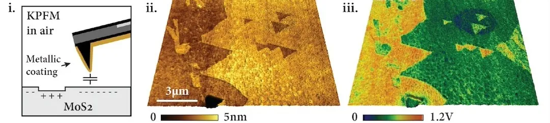
The KPFM measurement shown below was performed with a self-sensing Trilayer KPFM cantilever, on a few-layered molybdenum disulfide (MoS2) sample. The superposition of the topography and the work function reveals the surface potential between the layers.
In practice
How researchers use it
Example 1: Surface potential of few-layer MoS₂
(i) KPFM in air with a metal-coated tip. (ii) Topography of few-layer MoS₂, height scale 0 to 5 nm. (iii) Surface potential, scale 0 to 1.2 V. Credit: Hosseini et al., Nature Electronics 7, 567–575 (2024); use with permission
The study. A few-layered molybdenum disulfide (MoS₂) sample was measured by KPFM in air. Panel ii shows the topography (0 to 5 nm), panel iii the surface potential (0 to 1.2 V). The superposition of the topography and the work function reveals the surface potential between the layers.
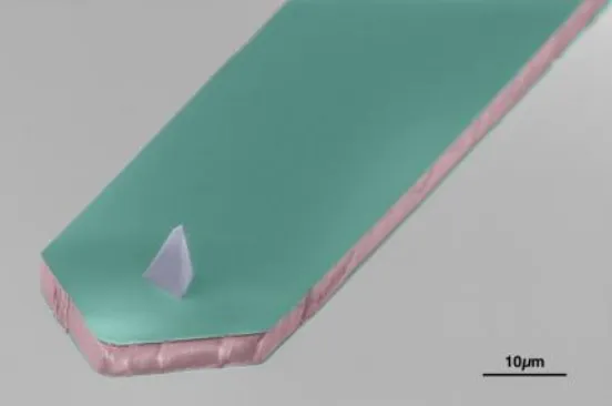
Where our cantilever is used. The measurement was performed with a self-sensing Trilayer KPFM cantilever. Its metal-coated tip is the Kelvin probe, and its integrated sensor provides the deflection signal for the KPFM feedback.
False-colour SEM image of the tip end of a metal-coated Trilayer cantilever. Scale bar 10 µm. Credit: c-sense
N. Hosseini et al., Nature Electronics 7, 567–575 (2024), doi:10.1038/s41928-024-01195-z. Figure from this paper, not open access: use with permission.
Example 2: A metallic tip as a movable gate for quantum emitters at 4 K
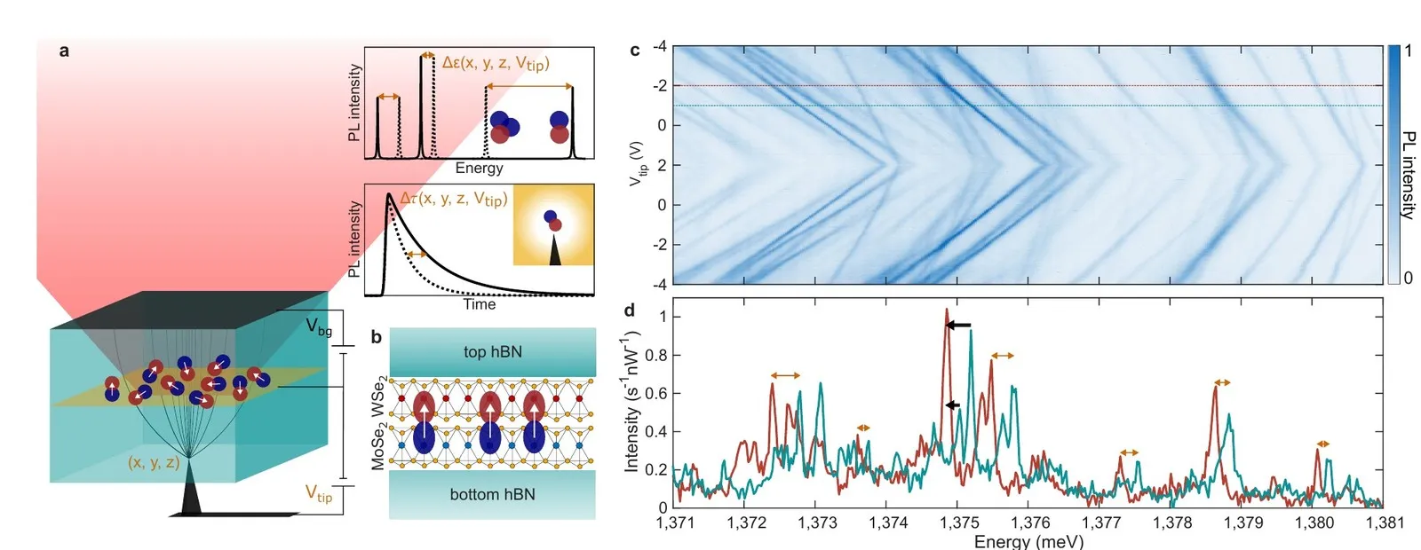
(a) A metallic tip in contact with the sample shifts the emission of individual quantum emitters. (b) The MoSe₂/WSe₂ bilayer between hBN layers. (c) Emission energy as a function of tip voltage. (d) Emission spectra at two tip voltages. Credit: Lyu, Vento et al., arXiv:2608.28574 (2026)
The study. The Quantum Matter Physics group at the University of Geneva combined cryogenic optical spectroscopy with scanning probe microscopy to study quantum emitters (interlayer excitons) in MoSe₂/WSe₂ bilayers. The electric field of a sharp tip shifts the emission of individual emitters. This separates emitters only a few tens of nanometres apart and controls their charge state.
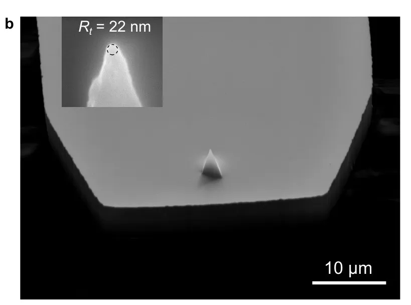
Where our cantilever is used. A c-sense KPFM cantilever with a 100 nm Pt-coated tip, operated with the NanoOne starter kit, is the movable gate. The tip stays in contact with the sample at 4 K, and the piezoresistive signal of the cantilever is used to hold the contact force constant during the scans. The cantilever brings no laser of its own into the optical experiment.
SEM image of the self-sensing cantilever with its conductive tip. Inset: the tip apex with a radius of about 22 nm. Scale bar 10 µm. Credit: Lyu, Vento et al., arXiv:2608.28574 (2026); use with the authors' permission
B. Lyu, V. Vento et al., arXiv:2608.28574 (2026). Figure: use with the authors' permission.